Overview of RF-NANO
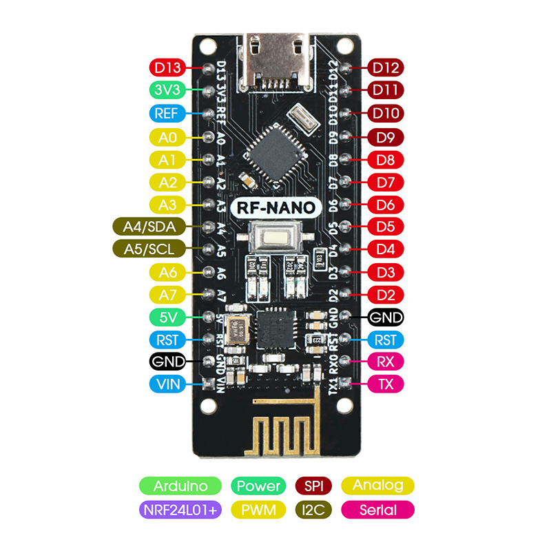
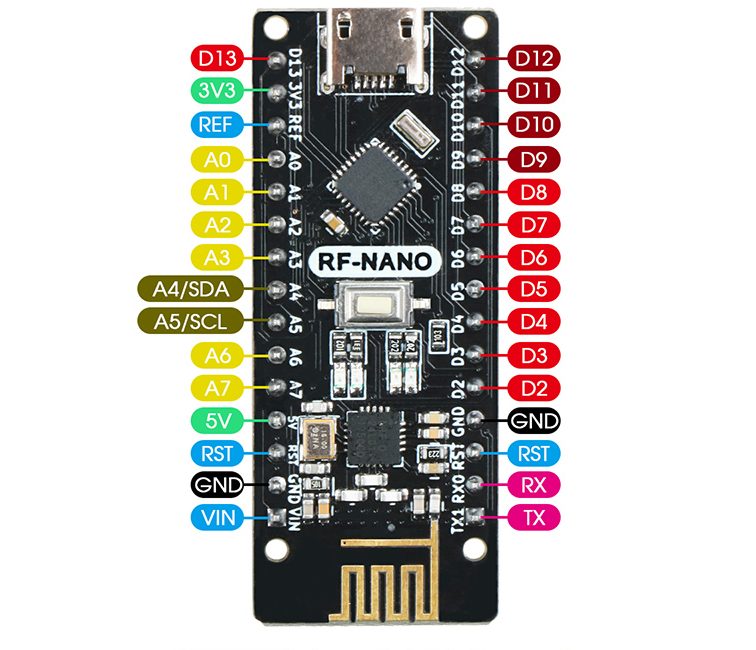
The NRF24L01+ chip is integrated on the RF-NANO board, which makes it have unlimited transceiver functions, which is equivalent to combining an ordinary Nano board and an NRF24L01 module into one, which is more convenient to use and small in size. The RF-NANO has exactly the same pins as the common Nano board, which is easy to transplant.
Introduction of RF-NANO Processor
Arduino RF-NANO microprocessor is ATmega328 (Nano3.0) with USB-Micro interface, 14 digital input/output ports (6 of which can be used as PWM output), 8 analog inputs, and a 16MHz crystal oscillator , a USB-Micro port, an ICSP header and a reset button. * Processor: ATmega328 * Operating voltage: 5V * Input voltage (recommended): 7-12V * Input voltage (range): 6-20V * Digital IO pins: 14 (6 of which are used as PWM outputs) (D0~D13) * Analog input pins: 6 (A0~A5) * IO pin DC current: 40mA * Flash Memory: 32KB (2KB of which is used for bootloader) * SRAM: 2KB * EEPROM: 1KB (ATmega328) * USB to serial port chip: CH340 * Working Clock: 16MHZ
Power Supply
Arduino RF-Nano power supply mode: Micro – USB interface power supply and external vin connected to 7~12V external DC power supply
Memory
ATmega328 includes on-chip 32KB Flash, of which 2KB is used for Bootloader. There are also 2KB SRAM and 1KB EEPROM.
Input Output
14 digital input and output ports: The working voltage is 5V, and each channel can output and access the maximum current of 40mA. Each channel is configured with a 20-50K ohm internal pull-up resistor (not connected by default). In addition to this, some pins have specific functions.Serial port signal RX (No. 0), TX (No. 1): Provide the serial port receiving signal of TTL voltage level, and connect with the corresponding pin of FT232Rl.
External interrupt (No. 2 and No. 3): Trigger the interrupt pin, which can be set to trigger on the rising edge, falling edge or both.
Pulse width modulation PWM (3, 5, 6, 9, 10, 11): Provide 6 8-bit PWM outputs.
SPI (10(SS), 11(MOSI), 12(MISO), 13(SCK)): SPI communication interface.
LED (No. 13): Arduino is specially used to test the reserved interface of the LED. When the output is high, the LED is turned on, otherwise, the LED is off when the output is low.
6 channels of analog input A0 to A5: each channel has a resolution of 10 bits (that is, the input has 1024 different values), the default input signal range is 0 to 5V, and the upper limit of the input can be adjusted through AREF. In addition to this, some pins have specific functions.
TWI interface (SDA A4 and SCL A5): support communication interface (compatible with I2C bus).
AREF: The reference voltage of the analog input signal.
Reset: Reset the microcontroller chip when the signal is low.
Communication Interface
Serial port: The built-in UART of ATmega328 can communicate with the external serial port through digital ports 0 (RX) and 1 (TX).
Communication between ATmega328 and NRF24L01+
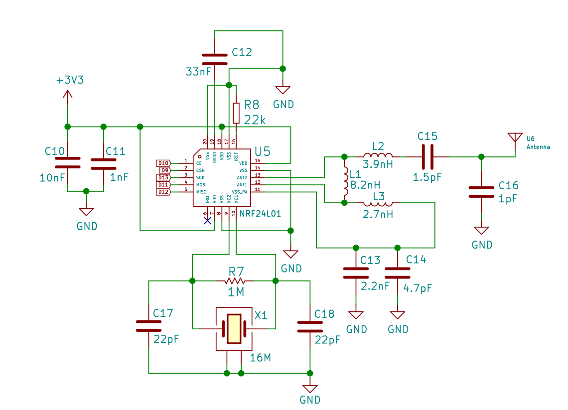
ATmega328 and NRF24L01+ are SPI communication, the schematic diagram is shown in the figure:

ATmega328 and NRF24L01+ chip pin connections:
ATmega328 chip NRF24L01+ chip
+3.3V VCC
GND GND
D9 CSN
D10 CE
D11 MOSI
D12 MISO
D13 SCK
Note: The D9, D10, D11, D12, D13 pins that have been occupied by ATmega328 can no longer be reused.
Downloader
The MCU on the Arduino RF-Nano has a preset bootloader program, so the program can be downloaded directly through the Arduino IDE software. You can also directly download the program to the MCU through the ICSP header on the RF-Nano.
Points to Note
The Arduino RF-Nano provides an automatic reset design that can be reset by the host. In this way, the software can be automatically reset in the RF-Nano through the Arduino software, and there is no need to press the reset button.
How RF-NANO works
Introduction to the working principle of RF-NANO
RF-NANO can transmit data as well as receive data.
When transmitting data: First configure NRF24L01+ to transmit mode: then write the receiving node address TX_ADDR and valid data TX_PLD into the NRF24L01+ buffer area from the SPI port according to the timing, TX_PLD must be written continuously when CSN is low, and TX_ADDR is written when transmitting Enter once, and then set CE to high level and keep it for at least 10μs, and then transmit data after a delay of 130μs; if the automatic response is turned on, then NRF24L01+ will enter the receiving mode immediately after transmitting data, and receive the response signal (the automatic response receiving address should be the same as the receiving address). The node address TX_ADDR is the same). If a response is received, the communication is considered successful, TX_DS is set high, and TX_PLD is cleared from the TX FIFO; if no response is received, the data is automatically retransmitted (automatic retransmission is enabled), ) reaches the upper limit, MAX_RT is set high, and the data in the TX FIFO is reserved for the next retransmission; when MAX_RT or TX_DS is set high, the IRQ becomes low, an interrupt is generated, and the MCU is notified. When the last transmission is successful, if CE is low, the NRF24L01+ enters idle mode 1; if there is data in the transmission stack and CE is high, it enters the next transmission; if there is no data in the transmission stack and CE is high, it enters idle mode 2.
When receiving data: First configure the NRF24L01+ to receive mode, then delay 130μs to enter the receive state and wait for the arrival of data. When the receiver detects a valid address and CRC, it stores the data packet in the RX FIFO, and at the same time, the interrupt flag bit RX_DR is set high, the IRQ becomes low, an interrupt is generated, and the MCU is notified to fetch the data. If the automatic response is turned on at this time, the receiver will enter the transmitting state at the same time and return the response signal. When the last reception is successful, if CE becomes low, the NRF24L01+ enters idle mode 1.
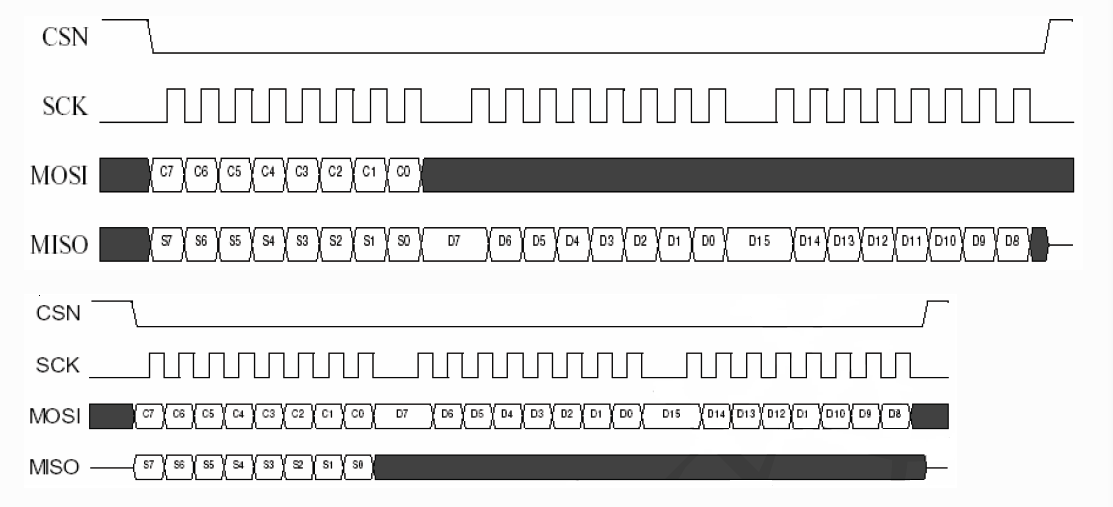
Be sure to enter standby mode or power-down mode before writing to the registers. the SPI operation and timing diagram are given

configuration word
The SPI port is a synchronous serial communication interface with a maximum transmission rate of 10 Mb/s. During transmission, the low-order byte is transmitted first, and then the high-order byte is transmitted. But for a single byte, the high bit must be sent first and then the low bit. There are 8 instructions related to SPI, and these control instructions are input by MOSI of NRF24L01+ when used. Corresponding status and data information is output from MISO to MCU.
All configuration words of nRF24L0l+ are defined by configuration registers, which can be accessed through the SPI port. There are 25 configuration registers in NRF24L01+, and the commonly used configuration registers are shown in Table 2.
Table 2: Common Configuration Registers
| Add | Name | Function |
|---|---|---|
| 00 | CONFIG | Set the working mode of NRF24L01+ |
| 01 | EN_AA | Set receive channel and auto answer |
| 02 | EN_RXADDR | Enable receive channel address |
| 03 | SETUP_AW | Set address width |
| 04 | SETUP_RETR | Set the time and times to automatically resend data |
| 07 | STATUS | Status register, used to determine the working status |
| 0A~0F | RX_ADDR_P0~P5 | Set receive channel address |
| 10 | TX_ADDR | Set the receiving contact address |
| 11~16 | RX_PW_P0~P5 | Set the effective data width of the receive channel |
Address Register Name Function
00 CONFIG Set the working mode of NRF24L01+
01 EN_AA Set the receiving channel and automatic answering
02 EN_RXADDR Enable receive channel address
03 SETUP_AW Set address width
04 SETUP_RETR Set the time and times of automatic data retransmission
07 STATUS status register, used to determine the working status
0A~0F RX_ADDR_P0~P5 Set receive channel address
10 TX_ADDR Set receive contact address
11~16 RX_PW_P0~P5 Set the effective data width of the receive channel
The working mode of RF-NANO
There is a state machine inside the NRF24L01+ chip, which controls the transition of the chip between different working modes. NRF24L01+ can be configured as Shutdown, Standby, Idle-TX, TX and RX five working modes.
Shutdown working mode:
In Shutdown working mode, all transceiver function modules of NRF24L01+ are turned off, the chip stops working, and consumes the least current, but all internal register values and FIFO values remain unchanged, and the registers can still be read and written through SPI. Set the value of the PWR_UP bit of the CONFIG register to 0, and the chip returns to the Shutdown working mode immediately.
Standby working mode:
In Standby mode, only the crystal oscillator circuit works, which ensures that the chip can start up quickly while consuming less current. Set the value of the PWR_UP bit in the CONFIG register to 1, and the chip will enter Standby mode after the clock is stable. The clock stabilization time of the chip is generally 1.5~2ms, which is related to the performance of the crystal oscillator. When pin CE=1, the chip will enter Idle-TX or RX mode from Standby mode, and when CE=0, the chip will return to Standby mode from Idle-TX, TX or RX mode.
Idle-TX working mode:
In the Idle-TX working mode, the crystal oscillator circuit and the clock circuit work. Compared to Standby mode, the chip consumes more current. When the transmitter TX FIFO register is empty and pin CE=1, the chip enters into Idle-TX mode. In this mode, if a new data packet is sent to the TX FIFO, the circuit inside the chip will start immediately and switch to the TX mode to send the data packet. In Standby and Idle-TX operating modes, all internal register values and FIFO values remain unchanged, and registers can still be read and written through SPI.
TX working mode:
When you need to send data, you need to switch to the TX working mode. The conditions for the chip to enter the TX working mode are: there is data in the TX FIFO, the value of the PWR_UP bit in the CONFIG register is 1, the value of the PRIM_RX bit is 0, and there is a high pulse on pin CE that lasts at least 10us. The chip will not directly switch from Standby mode to TX mode, but immediately switch to Idle-TX mode, and then automatically switch to TX mode from Idle-TX mode. The time to switch from Idle-TX mode to TX mode is between 120us and 130us, but will not exceed 130us. After a single packet of data is sent, if CE=1, the working mode of the chip is determined by the state of the TX FIFO. When there is data in the TX FIFO, the chip continues to remain in the TX working mode and sends the next packet of data; when If there is no data in the TX FIFO, the chip returns to Idle-TX mode; if CE=0, it returns to Standby mode immediately. After the data transmission is completed, the chip generates a data transmission completion interrupt.
RX working mode:
When it needs to receive data, it needs to switch to RX working mode. The conditions for the chip to enter the RX working mode are: set the value of the PWR_UP bit of the register CONFIG to 1, the value of the PRIM_RX bit to 1, and the pin CE=1. The time for the chip to switch from Standby mode to RX mode is 120~130us. When the address of the received data packet is the same as the address of the chip, and the CRC check is correct, the data will be automatically stored in the RX FIFO, and a data reception interrupt will be generated. The chip can store up to three valid data packets at the same time. When the FIFO is full, the received data packets are automatically discarded. In receive mode, the received signal power can be detected through the RSSI register. When the received signal strength is greater than -60dBm, the value of the RSSI bit in the RSSI register will be set to 1. Otherwise, RSSI=0. There are two ways to update the RSSI register: when a valid data packet is received, the RSSI will be automatically updated, and the RSSI will also be automatically updated when the chip is switched from RX mode to Standby mode. The value of RSSI varies with temperature within ±5dBm.
